
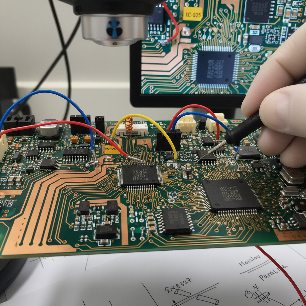

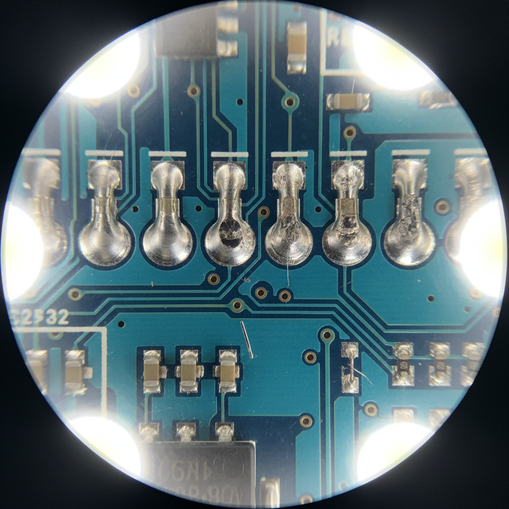
Every board reviewed before
the first stencil is cut.
NPI engineers run every new design through a 47-point DFM checklist before a stencil quote is issued. We catch paste aperture ratio violations, missing fiducials, and marginal annular rings at the data stage — not on the production floor at 2 a.m.
First-article builds include full IPC-A-610 Class 3 inspection with photographic documentation of every solder joint. NPI packages ship with a complete build dossier: reflow profile, paste lot, placement program revision, and AOI report.
- Minimum annular ring ≥ 0.15 mm per IPC-2221
- Copper-to-edge clearance ≥ 0.3 mm
- Paste aperture area ratio ≥ 0.66 for fine-pitch
- Thermal relief on all through-hole power pads
- Fiducial marks on all SMT layers
- Component keepout zones respected around connectors
- Test point access for every net (ICT compliance)
- Silkscreen clearance ≥ 0.1 mm from solder mask
+ 39 additional checks in full PDF
Reflow profiles tuned
to the tenth of a degree.
Our SMT line runs dual-gantry placement at 12,000 components per hour with SPI (solder paste inspection) after every print cycle. Approximately 70% of solder defects originate at the printing stage — so that's where we focus measurement effort.
NPI engineers profile every new board with thermocouples attached to BGAs, passives, and thermal mass components simultaneously. Baseline profiles are stored and reused; most assemblies fall within one of six established thermal envelopes within the first article run.

| Placement Speed | 12,000 CPH |
| Minimum Component | 01005 (0402 metric) |
| Fine Pitch IC | 0.3 mm pitch BGA |
| Stencil Printing | ±12.5 µm accuracy |
| Reflow Peak Temp | 230–245°C |
| Reflow Zones | 10 independent zones |
| Time Above Liquidus | 60–90 seconds |
| Cool Rate | 2–4°C / second |
| Board Thickness | 0.4 mm – 4.0 mm |
| Max Board Size | 508 × 508 mm |
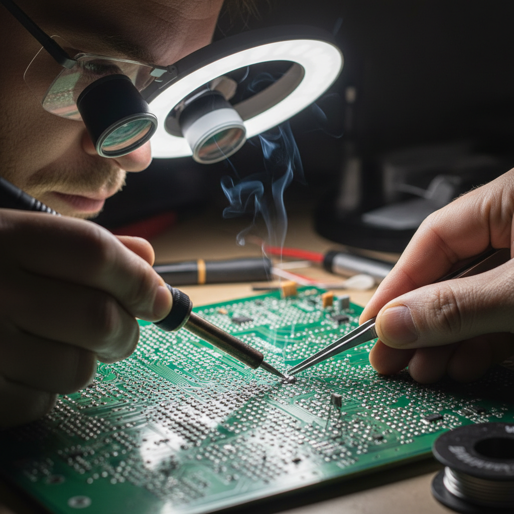
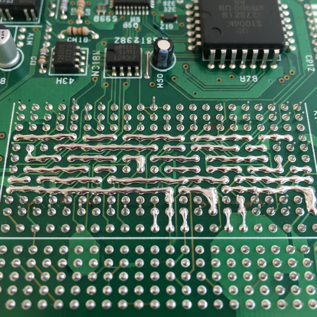
From bare board to
boxed, tested product.
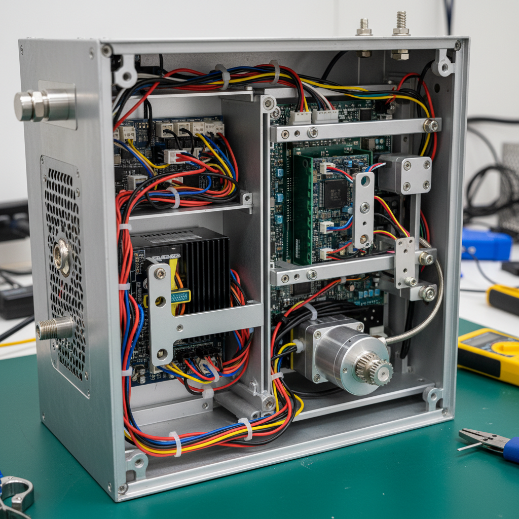
Not every design is 100% SMT. Odd-form connectors, high-current through-hole components, and press-fit pins require human hands and calibrated equipment. Our IPC-certified operators handle the full spectrum — from selective solder to complete box builds with cable routing and mechanical integration.
Nothing ships without
a pass record attached.
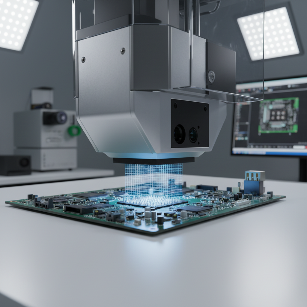
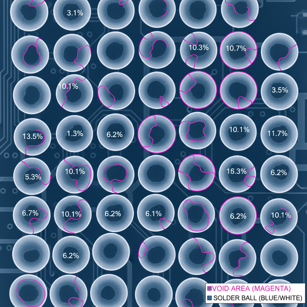
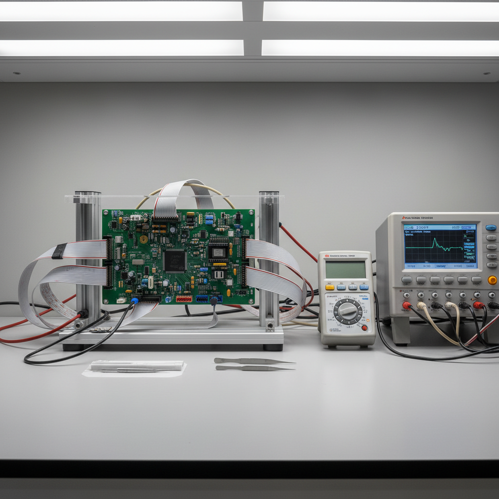
IPC Class 3 demands zero-tolerance for defects and 100% inspection at each stage. We run AOI post-reflow, AXI on every BGA and hidden-joint package, ICT for net-level parametric verification, and customer-defined functional test before any board is released to packing.
Every board that leaves this facility carries a serialized test record: equipment ID, operator, timestamp, and pass/fail result for every test step. Medical and defense builds include full environmental stress screening with thermal cycling logs.
| Method | Coverage |
|---|---|
| AOI Automated Optical Inspection | 100% post-reflow |
| AXI Automated X-Ray Inspection | BGA, QFN, hidden joints |
| ICT In-Circuit Test | Net-level parametric |
| FCT Functional Circuit Test | Full power-on test |
| ESS Environmental Stress Screening | Thermal cycling ±60°C |
Hardware startups, medical OEMs,
IoT teams. All on the same line.
"We sent Assemble our Gerbers on a Tuesday. By Thursday we had a DFM report flagging three paste aperture issues we'd missed. First articles were perfect. For a hardware startup shipping their first 500 units, that kind of NPI support is the difference between a launch and a nightmare."
"Class 3 compliance isn't optional in our space — it's table stakes. Assemble's documentation package is the cleanest I've reviewed in 15 years of medical device procurement. Serialized test records, thermal profile logs, AOI reports per lot. Audit-ready from day one."
"We designed a brilliant IoT gateway but had never sourced a stencil in our lives. Assemble handled everything — BOM scrub, stencil design, SMT, functional test with our firmware. We went from Gerbers to boxed, tested units in under four weeks."